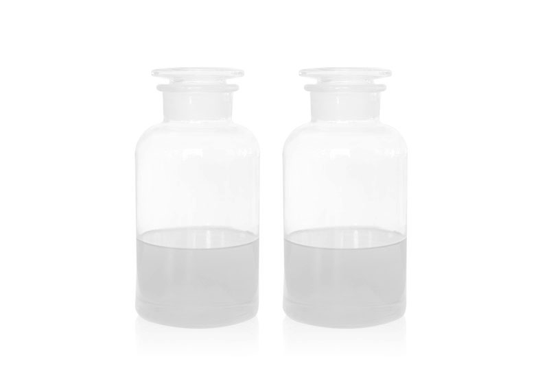
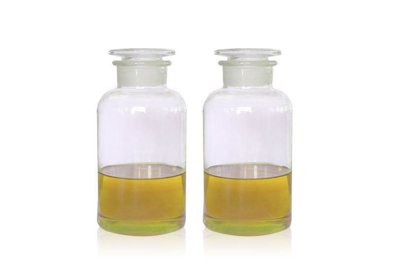
Etching solution TIN…
Repair etching solution for silicon wafer and IC lead frame.Characteristics:1. E…SUMII®︎
Etching solution NE-168, silicon wafer, IC substrate, and LED substrate can be selectively etched.
Characteristics:
1. Etching solution for etching nickel
2, silicon wafer, etchant used on IC substrate
3. Etchant for etching nickel without etching copper
Use:
Silicon wafer, IC substrate


Partners and end customers